Security Researcher, Cat Lover and Escape Room Aficionado!
Security Researcher, Cat Lover and Escape Room Aficionado!
04 May 2026
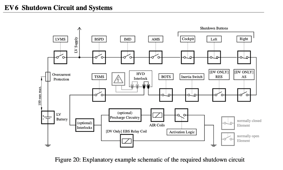
This project involved the design of an EV6-compliant shutdown circuit for a Formula Student AI (FS-AI) driverless electric racing car. The shutdown circuit is one of the most safety-critical systems in any Formula Student EV — its job is to ensure that the high-voltage accumulator is immediately and reliably isolated from the tractive system whenever any safety condition is violated.
The design was implemented in Altium Designer, moving from system-level schematic capture through to a fabricated, conformal-coated multi-layer PCB.
The shutdown circuit is a series chain of normally-open (NO) and normally-closed (NC) contacts wired through the low-voltage supply to the AIR (Accumulator Isolation Relay) coil activation logic. If any element in the chain opens, the AIRs de-energise and disconnect the accumulator from the tractive system.
The implemented chain follows the Formula Student Germany EV rules and includes the following nodes in series:
| Node | Function |
|---|---|
| LVMS | Low Voltage Master Switch — manual isolation of the LV system |
| Overcurrent Protection | Fuse/breaker protecting the LV shutdown bus |
| BSPD | Brake System Plausibility Device — opens if brakes are applied hard while significant motor current flows (detects stuck throttle) |
| IMD | Insulation Monitoring Device — detects insulation faults between HV and chassis |
| AMS | Accumulator Management System — monitors cell voltages and temperatures; opens on any out-of-range condition |
| Cockpit Button | Driver-accessible emergency shutdown, latching |
| Left / Right Buttons | External shutdown buttons on both sides of the car (marshals) |
| TSMS | Tractive System Master Switch — external key-operated switch |
| HVD Interlock | High Voltage Disconnect interlock loop — opens if the HVD plug is removed |
| BOTS | Brake Over-Travel Switch — NC switch that opens if the brake pedal travels beyond its mechanical limit (brake failure) |
| Inertia Switch | Opens on significant impact, preventing post-crash HV exposure |
For the FS-AI driverless class, two additional nodes are inserted into the chain:
Additionally, the driverless rules require an EBS (Emergency Brake System) relay coil in the circuit. When the shutdown chain opens, the EBS relay drops out and applies the brakes autonomously — critical since there is no driver to brake the car.
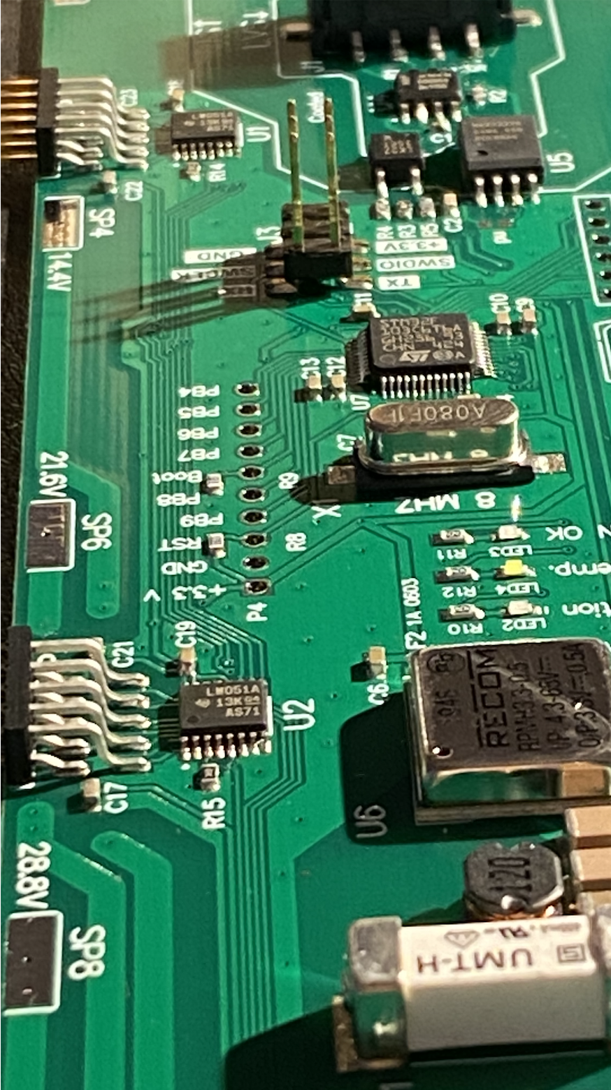
The PCB implements the activation logic and monitoring side of the shutdown system. Key design decisions:
The board operates from the car’s LV battery and requires an isolated supply for sections that interface with the HV-adjacent signals (IMD, AMS outputs). A RECOM switching DC-DC converter (UMT-H package, visible in the top-right of the PCB) provides this isolated rail, keeping the logic-side ground separated from the chassis ground reference used by the HV system.
Multiple solder-pad test points are exposed on the board for in-car diagnostics and pre-scrutineering checks:
These allow the team to probe the accumulator state through the LV system without exposing HV test equipment.
An on-board microcontroller (clocked at 8 MHz via crystal oscillator) manages:
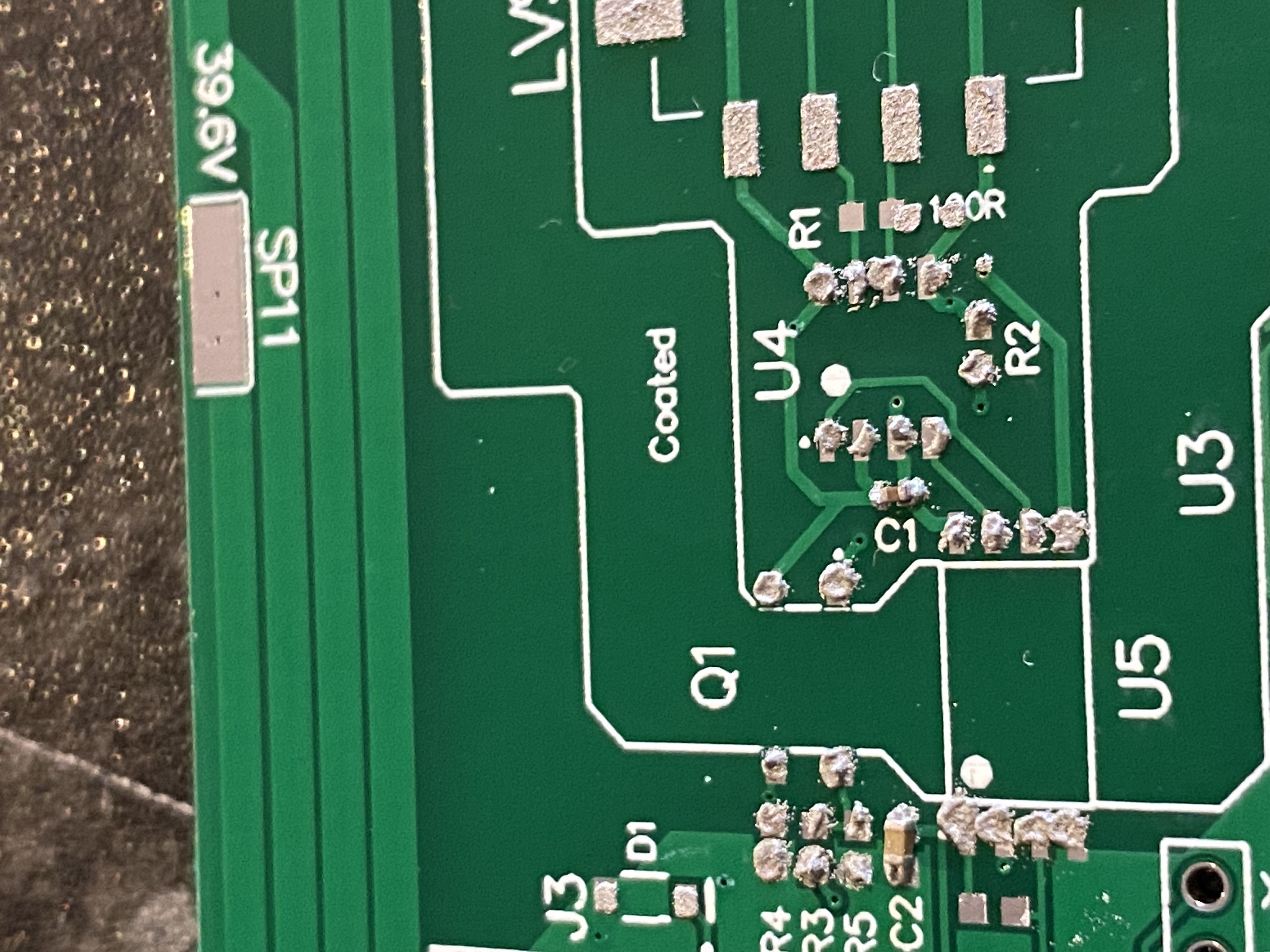
The output stage (bottom section of the PCB) drives the AIR coil and EBS relay. Visible components include:
The board is labelled “Coated” in the MOSFET output region — conformal coating was applied here to protect against moisture and vibration-induced failures during racing conditions.
The completed board was fabricated as a multi-layer PCB, assembled, and integrated into the FS-AI car’s electrical system. The shutdown chain was verified against the Formula Student rules checklist, with each node individually tested for correct open/close behaviour before the car was presented at scrutineering.